

為了得到我們網站最好得體驗效果,我們建議您升級到最新版本的Internet Explorer,或選擇另壹個web瀏覽器,壹個列表最流行的web瀏覽器在下面可以找到
您可在此下載主流瀏覽器:

Google Chrome

Firefox

IE11
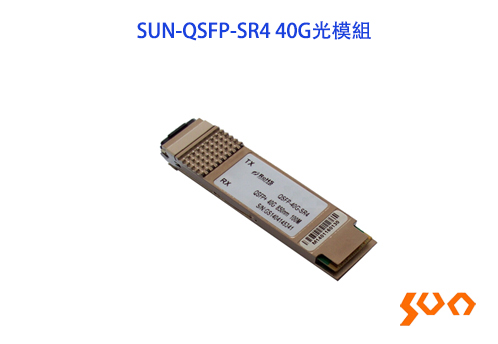
Suitable for mutilmode OM3 Max distance 100m, OM4 Max 150m.

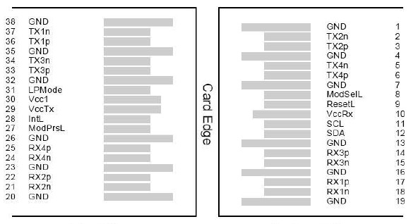
| PIN | Logic | Symbol | Name/Description | Notes |
| 1 | GND | Ground | 1 | |
| 2 | CML-I | Tx2- | Transmitter Inverted Data Input | |
| 3 | CML-I | Tx2+ | Transmitter Non-Inverted Data Input | |
| 4 | GND | Ground | 1 | |
| 5 | CML-I | Tx4- | Transmitter Inverted Data Input | |
| 6 | CML-I | Tx4+ | Transmitter Non-Inverted Data Input | |
| 7 | GND | Ground | 1 | |
| 8 | LVTLL-I | MODSEIL | Module Select | 2 |
| 9 | LVTLL-I | ResetL | Module Reset | 2 |
| 10 | VccRx | +3.3V Power Supply Receiver | ||
| 11 | LVCMOS-I/O | SCL | 2-Wire Serial Interface Clock | 2 |
| 12 | LVCMOS-I/O | SDA | 2-Wire Serial Interface Data | 2 |
| 13 | GND | Ground | 1 | |
| 14 | CML-O | Rx3+ | Receiver Non-Inverted Data Output | |
| 15 | CML-O | Rx3- | Receiver Inverted Data Output | |
| 16 | GND | Ground | 1 | |
| 17 | CML-O | Rx1+ | Receiver Non-Inverted Data Output | |
| 18 | CML-O | Rx1- | Receiver Inverted Data Output | |
| 19 | GND | Ground | 1 | |
| 20 | GND | Ground | 1 | |
| 21 | CML-O | Rx2- | Receiver Inverted Data Output | |
| 22 | CML-O | Rx2+ | Receiver Non-Inverted Data Output | |
| 23 | GND | Ground | 1 | |
| 24 | CML-O | Rx4- | Receiver Inverted Data Output | 1 |
| 25 | CML-O | Rx4+ | Receiver Non-Inverted Data Output | |
| 26 | GND | Ground | 1 | |
| 27 | LVTTL-O | ModPrsL | Module Present | |
| 28 | LVTTL-O | IntL | Interrupt | 2 |
| 29 | VccTx | +3.3 V Power Supply Transmitter | ||
| 30 | Vcc1 | +3.3 V Power Supply | ||
| 31 | LVTTL-I | LPMode | Low Power Mode | 2 |
| 32 | GND | Ground | 1 | |
| 33 | CML-I | Tx3+ | Transmitter Non-Inverted Data Input | |
| 34 | CML-I | Tx3- | Transmitter Inverted Data Input | |
| 35 | GND | Ground | 1 | |
| 36 | CML-I | Tx1+ | Transmitter Non-Inverted Data Input | |
| 37 | CML-I | Tx1- | Transmitter Inverted Data Input | |
| 38 | GND | Ground | 1 |
| Parameter | Symbol | Min | Max | Units |
| Storage Temperature | Tst | -20 | 85 | ºC |
| Input Voltage | Vin | -0.3 | Vcc+0.3 | V |
| Power Supply Voltage | Vcc | -0.3 | 3.6 | V |
| Relative Humidity (non-condensation) | RH | 5 | 95 | % |
| Parameter | Symbol | Min | Typical | Max | Units | |
| Operating Temperature | Non-industrial | Tc | 0 | 70 | ºC | |
| Industrial | Tc | -40 | 85 | ºC | ||
| Power Supply Voltage | Vcc | 3.13 | 3.3 | 3.47 | V | |
| Date Rate Each Lane | fd | 10.3 | 10.5(1) | Gbps | ||
| Power Dissipation | Pm | 1.5 | W | |||
| Fiber Bend Radius | Rb | 3 | CM | |||
| Parameter | Symbol | Min | Typical | Max | Units |
| Differential Input Impedance | Zin | 90 | 100 | 110 | Ohm |
| Differential Output Impedance | Zout | 90 | 100 | 110 | Ohm |
| Differential Input Voltage Amplitude | ΔVin | 300 | 1100 | mVp-p | |
| Differential Output Voltage Amplitude | ΔVOut | 500 | 800 | mVp-p | |
| Skew | Sw | 300 | ps | ||
| Bit Error Rate | BER | E-12 | |||
| Input Logic Level High | VIH | 2 | VCC | V | |
| Input Logic Level Low | VIL | 0 | 0.8 | V | |
| Output Logic Level High | VOH | VCC-0.5 | VCC | V | |
| Output Logic Level Low | VOL | 0 | 0.4 | V |
| Parameter | Symbol | Min | Typical | Max | Units | Notes |
| Transmitter | ||||||
| Center Wavelength | λC | 840 | 850 | 860 | nm | |
| RMS Spectral Width | ∆λ | 0.65 | nm | |||
| Average Launch Power Each Lane | Pavg | -7.5 | 2.5 | dBm | ||
| Difference in Launch Power between any Two Lanes (OMA) |
4 | dBm | ||||
| Extinction Ratio | ER | 3 | dB | |||
| Peak Power Each Lane | 4 | dBm | ||||
| Transmitter and Dispersion Penalty (TDP) Each Lane |
TDP | 3.5 | dB | |||
| Transmitter Eye Mask Definition {X1, X2, X3, Y1, Y2, Y3} | {0.23, 0.34, 0.43, 0.27, 0.35, 0.4} | Hit Ratio = 5x10⁻⁵ | ||||
| Average Launch Power OFF Transmitter Each Lane | -30 | dB | ||||
| Receiver | ||||||
| Center Wavelength | λC | 840 | 850 | 860 | Nm | |
| Minimum Average Received Power Each Lane | -9.5 | dBm | ||||
| Receiver Reflectance | Rr | -12 | dB | |||
| Maximum Average Received Power Each Lane | 2.4 | dBm | ||||
| Stressed Receiver Sensitivity (OMA) Each Lane | -5.4 | dBm | 1 | |||
| Peak Power Each Lane | 4 | dBm | ||||
| LOS Assert | LOSA | -30 | dBm | |||
| LOS De-Assert-OMA | LOSD | -7.5 | dBm | |||
| LOS Hysteresis | LOSH | 0.5 | dB | |||
| 型號 | 名稱 | 描述 |
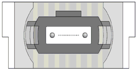
| SUN-QSFP-40G-SR4 | 光模組 | QSFP+SR4,40Gbps;OM3最大傳輸100m,OM4最大傳輸150m;非工業級 |
| SUN-QSFP-40G-SR4-I | 光模組 | QSFP+SR4,40Gbps;OM3最大傳輸100m,OM4最大傳輸150m;工業級 |
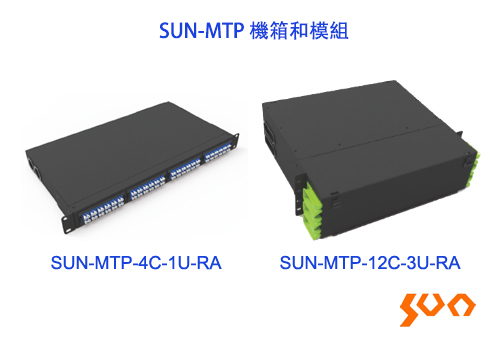
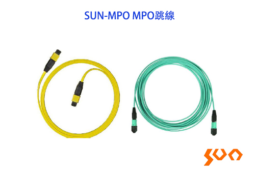
SUN-MTP 主機殼和模組
/型號:SUN-MTP
MTP機箱和模塊,用於MTP跳線的連接
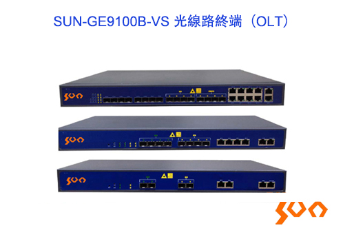
SUN-GE9100B-VS 光線路終端(OLT)
/型號:SUN-GE9100B-VS
1U的機架上提供2/4/8個PON口,最大可提供512路(1:64分路比情況下)ONU接入
Features
 1U設備佔用空間小,安裝維護方便 最大提供16個下聯EPON口、8個千兆上聯光口和8個千兆上聯網口
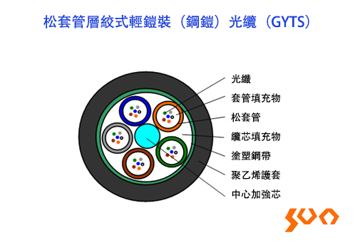
SUN-OC-SLT-SP GYTS光纜
/型號:SUN-OC-SLT-SP
GYTS室外光纜,束管層絞,金屬加強芯,單鋼鎧單PE護套
Features
具有良好的機械性能和溫度特性 松套管材料具有良好的耐水解性能和較高的強度 良好的抗壓性和柔軟性 鋼絲中心加強芯保證光纜的抗拉強度 塗塑鋼帶(PSP)提高光纜的抗透潮能力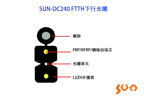
SUN-DC240 FTTH下行光纜
/型號:SUN-DC240
FTTH室內光纜(GJYXCH),蝶型,鋼絲/FRP/KFRP加強件,帶鋼絲自承,LSZH外被
Features
兩根平行加強芯使光纜具有良好的抗壓性能 單根鋼絲附加加強芯使光纜具有良好的抗拉性能 低煙無鹵外護套 光纜結構簡單、重量輕、實用性強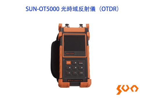
SUN-OT5000光時域反射儀(OTDR)
/型號:SUN-OT5000
OTDR,單模/多模,各種動態範圍,FC接口,SC/ST接口可選
Features
開機啟動時間短 FTTX線上測試(可穿通1:64分路器) 內置PON光功率計(用於三網測試)(只限“-PON”型號) 高配版配有穩定光源(LS)、普通光功率計(PM)、可視故障定位儀(VFL)和光纖端面檢測儀(MCI)模組 USB資料介面(可利用上位機軟體處理資料和輸出報告) 防塵、防震設計(通過2米跌落試驗) 重量輕、體積小、操作簡單、堅固耐用 形象直觀Link image軟體(選配)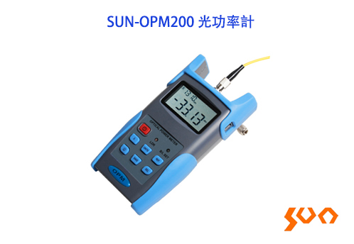
SUN-OPM200光功率計
/型號:SUN-OPM200
手持式光功率計,配合OPM200光源使用
Features
用戶自校準功能 線性(mW)和非線性(dBm)指標同時顯示 10分鐘無操作自動關機功能 標配FC/SC/ST可替換介面 背光顯示 REF定義(參考光功率記錄)功能 背光智慧控制 波長和頻率自動識別 大容量儲存空間,資料存儲可達1000條 USB傳輸功能,方便資料儲存入電腦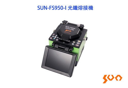
SUN-FS950-I光纖熔接機
/型號:SUN-FS950-I
饋線型熔接機
Features
適用於幹線光纜的熔接 PAS圖像數文書處理系統 9秒熔接時間、20秒加熱時間 多種光纖對準方式 5.7英寸彩色顯示大屏


 sun.telecom@msa.hinet.net
 +886 2 2222 9167
 paisanhsu
 Joycehsu68


 sun.telecom@msa.hinet.net
 +886 2 22229167
  臺灣新北市中和區中板路11號4樓